What is TSV?
TSV (Through-Silicon Via) is an advanced 3D integrated circuit packaging technology. By perforating the chip and filling the conductive material, it realizes the vertical connection within the chip, between the chip and the chip and the package. TSV technology can stack chips with different functions on top of each other to improve integration, reduce power consumption, and reduce the size of the chip package. TSV technology is widely used in various fields, such as microprocessor, memory, sensor, etc. It is one of the important technologies to promote the development of integrated circuit manufacturing technology to the three-dimensional direction.
Advantages of TSV
High integration: TSV technology can realize the vertical connection within the chip, between the chip and the chip and the package, so as to realize the stack combination of multiple chips, and improve the integration of the system.
Low power consumption: Because TSV technology can shorten the signal transmission distance, reduce the signal transmission delay, thereby reducing power consumption.
Miniaturization: TSV technology can reduce the size of the chip package, making the overall package more compact, which is conducive to achieving more functions in a limited space.
High performance: TSV technology can improve the communication speed and bandwidth between the various functional modules inside the chip, thereby improving the performance of the overall system.
Good heat dissipation: TSV technology can improve the heat dissipation effect of the chip, because the heat can be conducted more efficiently through the vertical connection.
Cost reduction: Although the cost of implementing TSV technology is higher, the overall cost of the system can be reduced due to the high integration and miniaturization that can be achieved.
In general, TSV technology has obvious advantages in improving integration, reducing power consumption, miniaturization, improving performance, good heat dissipation effect and reducing cost, and is an important development direction in the future integrated circuit packaging field.
Equipment problems in the development of TSV process technology
TSV technology was initially widely used in image sensors, but in the future will be further applied in logic chips, memory chips, cpus, and even heterogeneous integration, and its technical application fields continue to expand, and the outlook is very optimistic. With the continuous development of TSV technology, it will promote the development of new production equipment, such as deep corrosion equipment, copper filling equipment, bonding machines, microdetectors, etc., but also means that many traditional equipment will face elimination.
In recent years, China has made certain experience and breakthroughs in the field of deep etching, PVD/CVD, wafer thinning, wafer bonding and other equipment, but there is still a big gap compared with foreign levels. The key equipment required for the TSV process is dependent on a small number of foreign enterprises, resulting in high costs, long lead times, and slow responses to market changes. If the equipment of domestic equipment manufacturers can reach or even exceed the level of foreign equipment in economic and technical indicators, it is expected to gain broader market recognition and opportunities.
Therefore, domestic equipment manufacturers should continue to improve the technical level and product quality, increase technological innovation and research and development investment, in order to improve equipment performance and reduce costs, and better adapt to market demand. With the further popularization and application of TSV technology, the domestic equipment manufacturing industry is expected to make greater breakthroughs and development in this field and achieve better market prospects.
TSV process key process equipment
The TSV (Through-Silicon Via) fabrication process consists of several key steps, each of which is technically difficult and requires specific equipment to achieve. The following are the key steps and related equipment involved in the TSV manufacturing process:
1, through hole production: through the deep etching process to achieve. This step requires the use of deep Etching equipment, such as Ion Beam Etching System or Reactive Ion Etching System, usually using the Bosch process to achieve deep hole etching.
2, insulation layer, barrier layer and seed layer deposition: the use of chemical vapor deposition (CVD) or physical vapor deposition (PVD) equipment to achieve. It is important to ensure the uniformity and adhesion of the layers.
3, copper filling: by Electrochemical Deposition equipment to achieve, the need to avoid holes and other defects to ensure that the filled copper at high temperature to maintain normal electrical properties.
4, chemical mechanical polishing: used to remove excess metal to ensure smooth surface. Need to use chemical mechanical polishing equipment to achieve.
5, wafer thinning: In order to reduce the overall thickness, it is usually necessary to thin the wafer. This step is usually achieved using a Wafer Thinning Grinder or a chemical mechanical polishing device.
6, wafer bonding: Different chips or components are bonded, which can be achieved by wafer bonding equipment.
TSV production process involves a variety of equipment, such as deep etching equipment, PVD equipment, CVD equipment, electrochemical deposition equipment, chemical mechanical polishing equipment, wafer grinding machine, etc. The equipment involved in through hole fabrication, insulation/barrier/seed layer deposition, copper filling, wafer thinning and wafer bonding are critical in the process and directly affect the performance indicators and overall quality of the TSV. Therefore, the fine control and optimization of the equipment in these critical process steps is essential.
Deep silicon etching equipment
Deep reactive ion etching (DRIE) is a process commonly used to create through-silicon holes, and the common deep silicon etching technique is called the "Bosch" process, named after the company that originally invented it.
In the Bosch process, a standard cycle consists of two steps, selective etching and passivation. In the selective etching process, two gases SF6 and O2 are usually used, while C4F8 gas is used in the passivation process. First, SF6 plasma is used to etch the silicon substrate, then C4F8 plasma is deposited on the silicon substrate, and finally O2 plasma is added to these gases to effectively control the etching rate and selectivity. As a result of the alternating use of these steps, the Bosch process forms a shell-like etched side wall during the etching process.
In the Bosch process, a standard cycle consists of two steps, selective etching and passivation. In the selective etching process, two gases SF6 and O2 are usually used, while C4F8 gas is used in the passivation process. First, SF6 plasma is used to etch the silicon substrate, then C4F8 plasma is deposited on the silicon substrate, and finally O2 plasma is added to these gases to effectively control the etching rate and selectivity. As a result of the alternating use of these steps, the Bosch process forms a shell-like etched side wall during the etching process.
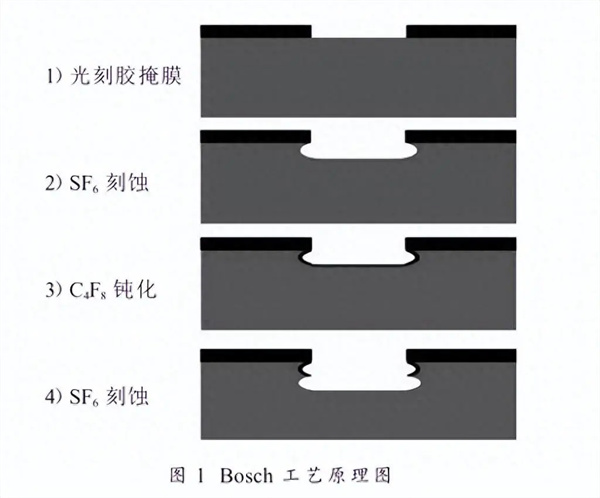
At present, deep silicon etching equipment is mainly controlled by American Applied Materials, Pan Forest Semiconductor and other equipment manufacturers. From the domestic point of view, in recent years, with the support of major national science and technology special projects, the deep silicon plasma etching machine developed by micro Semiconductor, North Microelectronics and other manufacturers can be put into the research and development and mass production of through-hole silicon etching. In particular, the DSE200 series etching machine is the first deep silicon plasma etching machine launched by North Microelectronics Company in 2012, which can achieve up to 50:1 silicon aspect ratio etching, and at the same time achieve excellent side wall shape control, stable uniformity, and extremely high etching selection ratio.
PVD/CVD deposition equipment
After the formation of through-silicon holes, a layer of insulating material SiO2 is often deposited on the inner surface of through-silicon holes by plasma enhanced chemical vapor deposition (PECVD), which is one of the mainstream technologies for preparing TSV (Through Silicon Via) hole insulation. The process is deposited at a lower temperature range (100 to 400 ° C).
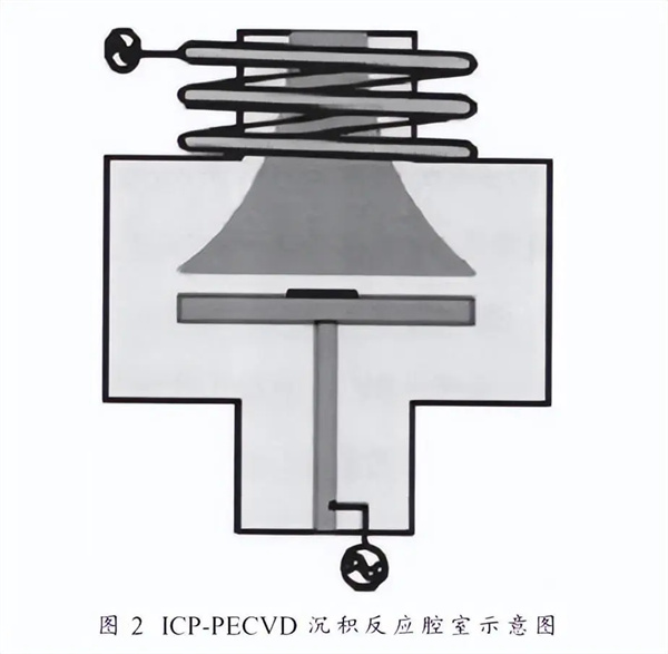
In recent years, a new type of plasma vapor enhanced chemical deposition device ICP-PECVD has been introduced to fill the insulation layer of TSV holes. Unlike conventional PECVD devices, ICP-PECVD devices inductively couple RF power to the process chamber, coupled with a RF source coupled to the reaction chamber substrate, to improve the directivity of the reactive ions. Typical ICP-PECVD process chamber design is shown in Figure 2. The temperature of SiO2 deposition by ICP-PECVD process can be reduced to 20 ~ 100 ℃, and the concentration of reactive ions is high, which is helpful to improve the filling efficiency of TSV holes.
In recent years, a new type of plasma vapor enhanced chemical deposition device ICP-PECVD has been introduced to fill the insulation layer of TSV holes. Unlike conventional PECVD devices, ICP-PECVD devices inductively couple RF power to the process chamber, coupled with a RF source coupled to the reaction chamber substrate, to improve the directivity of the reactive ions. Typical ICP-PECVD process chamber design is shown in Figure 2. The temperature of SiO2 deposition by ICP-PECVD process can be reduced to 20 ~ 100 ℃, and the concentration of reactive ions is high, which is helpful to improve the filling efficiency of TSV holes.
After the insulation is formed, a metal diffusion barrier and seed layer are usually deposited inside the TSV hole using physical vapor deposition (PVD) to prepare for the subsequent copper filling. If the filling material is polysilicon or tungsten, the seed layer is not required.
For subsequent electroplated copper filling, a continuous barrier layer and seed layer are required on the side wall and bottom of the TSV hole. The continuity and uniformity of the seed layer is considered to be one of the key factors affecting the quality of TSV copper filling. The characteristics of the seed layer will vary according to the shape of the TSV hole, the depth to width ratio and the deposition method. The deposition thickness, uniformity and adhesion strength of the seed layer are very important evaluation indexes.
For subsequent electroplated copper filling, a continuous barrier layer and seed layer are required on the side wall and bottom of the TSV hole. The continuity and uniformity of the seed layer is considered to be one of the key factors affecting the quality of TSV copper filling. The characteristics of the seed layer will vary according to the shape of the TSV hole, the depth to width ratio and the deposition method. The deposition thickness, uniformity and adhesion strength of the seed layer are very important evaluation indexes.
Electroplating copper filling equipment
Many cost models show that the TSV filling process is one of the more expensive steps in the entire process flow. One of the main yield losses of TSV is inadequately filled voids. As a suitable technology for filling through silicon holes, copper plating process has attracted much attention, especially for the full fill plating technology for TSV high aspect ratio (usually greater than 10:1).
Many foreign companies have successfully developed this technology and launched mature products, including NEXX, TECHNIC, Semitool and other companies. In particular, NEXX Company in the United States is a professional equipment supplier in the field of advanced packaging, and its Stratus S200 (4-8 inches), S300 (8-12 inches) automatic plating equipment has been applied in the world's major packaging manufacturers for the mass production of 12-inch and below specifications wafers. It can be applied to TSV, convex point, UBM, RDL, copper interconnect and other processes. As shown in Figure 3:
Many foreign companies have successfully developed this technology and launched mature products, including NEXX, TECHNIC, Semitool and other companies. In particular, NEXX Company in the United States is a professional equipment supplier in the field of advanced packaging, and its Stratus S200 (4-8 inches), S300 (8-12 inches) automatic plating equipment has been applied in the world's major packaging manufacturers for the mass production of 12-inch and below specifications wafers. It can be applied to TSV, convex point, UBM, RDL, copper interconnect and other processes. As shown in Figure 3:
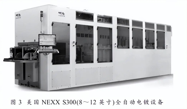
NEXX's range of electroplating equipment is sold worldwide, with Asian sealed-test manufacturers accounting for 75% of the market share. It is understood that the domestic packaging industry leader Changdian, Fujitsu, etc., widely used Stratus series equipment in their production lines. These equipment adopts shear plating technology, has the advantages of uniform coating, compact structure, easy to expand and so on, which provides a kind of automatic equipment with stable quality, high production efficiency and small footprint for sealed test manufacturers.
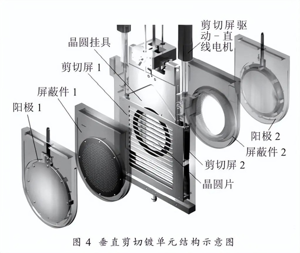
The core part of this series of devices is the vertical shear plating unit (as shown in Figure 4), which mainly includes components such as anode, shield, wafer fixture, shear screen and drive motor. These components are individually installed on the unit frame and include a mounting guide, a shear screen to improve coating uniformity and a DC conductive clamping mechanism. All the main components are made of fluoroplastic material, and the unit is assembled by connecting bolts and seals.
The core part of this series of devices is the vertical shear plating unit (as shown in Figure 4), which mainly includes components such as anode, shield, wafer fixture, shear screen and drive motor. These components are individually installed on the unit frame and include a mounting guide, a shear screen to improve coating uniformity and a DC conductive clamping mechanism. All the main components are made of fluoroplastic material, and the unit is assembled by connecting bolts and seals.
At present, domestic research institutions have obtained some research results on TSV individual technologies, but almost no manufacturers are involved in electroplating related process equipment, only the second Research Institute of China Electronics Technology Group Corporation is conducting research on TSV copper filling process technology, and has related experimental equipment delivered to customers.
Wafer thinning device
TSV requires wafers to be reduced to 50 μm or thinner to expose the copper at the bottom of the silicon hole in preparation for the next step of interconnection. At present, wafer thinning can be achieved by mechanical grinding, chemical mechanical polishing, wet and dry chemical treatment and other different processing processes, through the organic combination between them, and optimize the proportional relationship between these processes, to ensure that the wafer can be thinned to the required thickness, but also to have enough strength. The comparison of the four main wafer thinning methods is shown in Table 1.
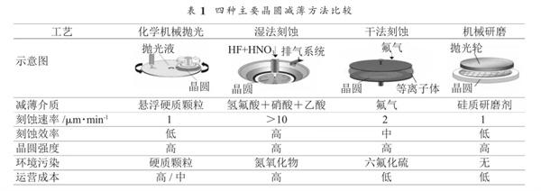
Under the requirement of a thin thickness of less than 50 μm, it is difficult to avoid wear and internal stress problems during the thinning process, and the rigidity of the wafer is difficult to maintain its original flat state. In addition, there are challenges in the transfer and transfer of wafers in subsequent processes. In order to solve these problems, the industry currently mainly uses all-in-one solutions, which integrate wafer grinding, polishing, removing protective film, pasting film and other processes in a single device. In this device, the wafer is always adsorbed on the vacuum suction cup, maintaining a flat state, thus solving the difficulties in the process of moving.
Figure 5 shows the basic configuration diagram of Tokyo Precision Corporation's all-in-one PG200/300. In this unit, the PG part integrates grinding and polishing functions. Through a large disc rotary table with four vacuum suckers, the wafer can be rotated clockwise 360° without leaving the vacuum suckers, and is sent to different processing stations such as rough grinding, fine grinding, polishing, etc., to complete the entire thinning process. The application of this all-in-one device effectively solves the technical problems in the wafer thinning process and improves the processing efficiency and quality.
Figure 5 shows the basic configuration diagram of Tokyo Precision Corporation's all-in-one PG200/300. In this unit, the PG part integrates grinding and polishing functions. Through a large disc rotary table with four vacuum suckers, the wafer can be rotated clockwise 360° without leaving the vacuum suckers, and is sent to different processing stations such as rough grinding, fine grinding, polishing, etc., to complete the entire thinning process. The application of this all-in-one device effectively solves the technical problems in the wafer thinning process and improves the processing efficiency and quality.
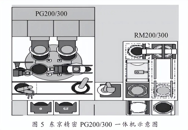
The transfer of the thinned wafer from the PG part to the RM part is usually done using a porous ceramic sucker. In the RM part, the removal of the protective film and the pasting of the scribing film are mainly carried out. Since the peeling of the protective film needs to be done on the front of the wafer, the wafer must be turned over. However, because the wafer thickness is very thin, the flipping process is very difficult.
In order to solve this problem, Tokyo Precision Company advanced the film placement process in the traditional film stripping process to support the wafer by using the flatness and tension of the sliced film when pasted to the frame. This method effectively solves the difficulties in the wafer flipping process and ensures the smooth progress of the subsequent process.
In order to solve this problem, Tokyo Precision Company advanced the film placement process in the traditional film stripping process to support the wafer by using the flatness and tension of the sliced film when pasted to the frame. This method effectively solves the difficulties in the wafer flipping process and ensures the smooth progress of the subsequent process.
Wafer bonding equipment
Wafer bonding was originally developed for MEMS manufacturing processes, primarily to enable wafer-level overlay technology. With the development of technology, wafer bonding is not only used to cover MEMS wafers, but also applied to stack wafers with different functions, achieving 3D stacking of wafers through TSV.
At present, wafer bonding uses a variety of methods, including direct oxide bonding, anode bonding, bonding, solder-based bonding, metal-metal direct bonding, ultrasonic bonding, glass medium bonding, etc. However, due to the limitation of the thermal budget of CMOS devices, the bonding processes compatible with CMOS wafers interconnected with TSV are mainly limited to direct oxide bonding, metallic bonding (Cu-Cu or Cu-Sn-Cu), adhesive bonding, and combinations of them.
Among these methods, Cu-Cu direct bonding has many advantages, such as low resistivity, good resistance to electromigration, and reduced interconnect resistance capacitance delay, while achieving mechanical and electrical contact interfaces.
However, achieving reliable Cu-Cu bonding remains a challenge for most applications, mainly due to its tendency to form natural oxides under high temperature, high pressure and long time processes, which adversely affects device reliability. Currently, one of the main bottlenecks in Cu-Cu direct bonding is the high process temperature, which negatively affects device reliability and manufacturing yield, and the high temperature also adversely affects the alignment accuracy between wafers.
In order to solve these problems, wafer bonding equipment supplier EVG Austria has developed an optical alignment, low temperature Cu-Cu hot pressing bonding process to achieve sub-micron alignment accuracy. This innovation brings new possibilities for the development of Cu-Cu bonding technology.
I-stock
I-stock has always adhered to the customer needs as the core, driven by intelligent equipment, precision technology, industrial software to open up data flow, data +AI algorithm to empower the electronics and semiconductor industry intelligent storage, focus on product quality, heart service. I-stock helps enterprises solve the practical problems encountered in the scientific, standardized, digitized, automated and intelligent upgrading of the intelligent storage field, and provides customized services for intelligent storage equipment. In the future,I-stock will continue to leverage its advantages in technical talent and resources to contribute to the transformation and upgrading of the manufacturing industry. In this process, iI-stock will help more HBM manufacturing enterprises to work together and jointly promote China's manufacturing industry to the top of the global value chain.


